What systems is Confed familiar with when it comes to PCB design?
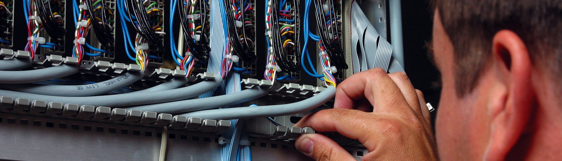
Convenience and evolution are making electrotechnical products increasingly complex to produce. Users expect more and more (electrotechnical) products that think "smart. The miniaturization of electronic components is also becoming increasingly important. As a result, among other things, the complexity of printed circuit boards (PCBs) is evolving.
For us, this is not a stumbling block. Confed has several systems for assembling the most complicated
PCBs to assemble and design. In this blog, we explain how we accomplish this.
How is a PCB design created
A PCB design requires a combination of different disciplines. Our specialists have knowledge and experience in designing PCBs and use different systems and techniques for realizing them. Confed uses different systems for the realization of a PCB design.
The different systems for PCB design at Confed
These different systems each have their own specialty that can solve any issue our customers may have. We briefly explain for each system, within our offering, what it entails and can do for you.
- High-density interconnect (HDI). This is a design characterized by its high density of components. This provides more interconnections and takes up minimal space. The design of HDI-PCBs is preferred to reduce overall cost.
- Multiboard. A multiboard PCB design follows the same process as that of a single board. However, components are added to the schematics for the boards.
- DDR3. Double-Data Rate or a DDR memory is very common today in PCB design. This is a type of ''synchronous dynamic random access memory'' (SDRAM) with a high-bandwidth interface ("double data rate").
- 12 layer. The 12 layer PCB provides the basis for a modern electronic circuit. The 12 Layer PCB is designed to withstand high temperatures and stressful conditions (e.g., automotive).
- Blind/Burried vias. A blind/burried vias connects exactly one outer layer to one or more inner layers. This technology provides more functionality in less board space.
- Length matching. This involves matching the lengths of two or more PCB traces as they are routed across a board.
- Diff pairs. This is a design technique (for PCBs) used to create a balanced transmission system that can carry differential signals across a circuit board.
- Controlled impedance. This is the characteristic impedance of a transmission line formed by PCB traces and associated reference planes. This method is often used when high-frequency signals multiply on PCB transmission lines.
- Flex Rigid. This is a hybrid of hardboard and flexible circuits. Among other things, these PCBs are easy to ''bend'' and adapt to a device.
- Would you like to learn more about what our systems do and which system best suits your PCB development needs? Feel free to contact us without obligation. We will look at all the possibilities for you.
Choose Confed. Choose fast, reliable and quality.
Got curious?
Have you become curious about what we can do for you in this area? We would like to invite you to contact us. This can easily be done by phone or via our general email address. You can also send us a request via the contact page and we will get back to you as soon as possible.
Contact via:
info@confed.eu or tel: +31(0) 33 454 1340