Shorten the product design cycle with Flying Probe Testing
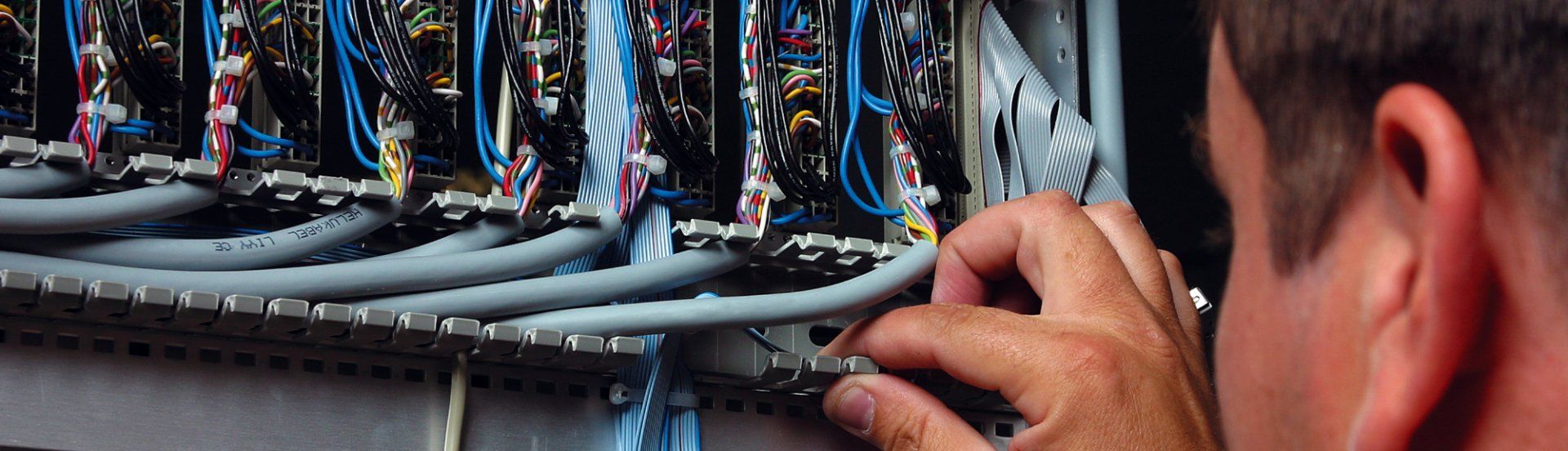
Before PCBs (Printed Circuit Boards) and PCB assemblies are delivered, they must pass various electrical tests. Electrical tests are conducted to ensure the qualitative and reliable performance of PCBs in final products. These tests are applied to detect problems early. Flying Probe Testing is the test of choice to shorten your product's time-to-market and product design cycle to the maximum extent possible. In this blog, we explain exactly how Flying Probe Testing works.
What is Flying Probe Testing?
A Flying Probe test, or a flying probe test, goes one step further than the Bed of Nails test. The Flying Probe test is a test in which a probe is mounted on a mechanical arm. The probe flies around the circuit board and uses a needle to test the various components of the board. Confed ensures the operation of each component of the circuit board, using tests such as the flying probe test.
How a Flying Probe Test Works
As the probe flies around the circuit board, the probe contacts test pads. In this way, defects can be detected quickly. A probe is in close contact with drivers via multiplexed systems and various sensors such as frequency counters and digital multimeters. The remaining components of the board are shielded during each Flying Probe Test. Defect detection is not interfered with in this way. A Flying Probe Test tests not only the resistance of components, but also the self-inductance of a component. The self inductance of an electrical component can create a violent counter voltage.
The advantages of Flying Probe Testing over Bed of Nails Testing
The Flying Probe testing technique has several advantages over the usual Bed of Nails technique. We briefly discuss the advantages.
- the Flying Probe method is cost-effective;
- the Flying Probe has a short test cycle;
- high conversion flexibility;
- rapid feedback from PCB design specialists during the prototype period.
A disadvantage of the Flying Probe Testing method is that the cost for large orders can increase. However, this method is very suitable for low-volume PCB production. The short test duration of the Flying Probe Test ensures that the PCB assembly process can be started within a short time. The short test duration is a big difference from the usual In-Circuit Testing method, the development of which can take up to several months in some cases.
Using Flying Probe Testing for PCB Assembly at Confed
PCB assemblies are often tested via In-Circuit Testing, or ICT. Flying Probe Testing is an efficient technique that we also employ at Confed. Electronic devices evolve by the day and require more extensive testing to ensure high quality. At Confed, we see the complexity and importance of keeping up with the latest developments. Our specialists have years of knowledge and experience that are continuously deployed to think along with our customers. We deploy tests such as the Flying Probe test technique for the most innovative end products. Would you like to know more about this testing technique or about the possibilities at Confed? Feel free to contact us for an informal introduction. We are happy to think along with you.
Choose Confed. Choose fast, reliable and quality.
Got curious?
Have you become curious about what we can do for you in this area? We would like to invite you to contact us. This can easily be done by phone or via our general email address. You can also send us a request via the contact page and we will get back to you as soon as possible.
Contact via:
info@confed.eu or tel: +31(0) 33 454 1340